- Ruhr-Universität Bochum

Transmission Electron Microscopy
My adventure with microstructural characterization started during my PhD studies in Poland. At that time, I was simply fascinated by the electron microscope itself: its complexity, performance, and possibility to „see atoms”. During one of the discussions with my supervisor - Prof. Henryk Morawiec, we read the text of Mr Robert W. Cahn: „Studies of the interface structure and properties are the most striking of all changes in the practice of materials science and engineering, which will certainly have a major impact on the future of our science...” [Materials Today, Vol 2, Elsevier 1999]. That citation becomes my scientific guidance and a gate into the wonders of materials science where the microscope is just a tool to understand the materials through the study of their microstructure and its correlation with properties.
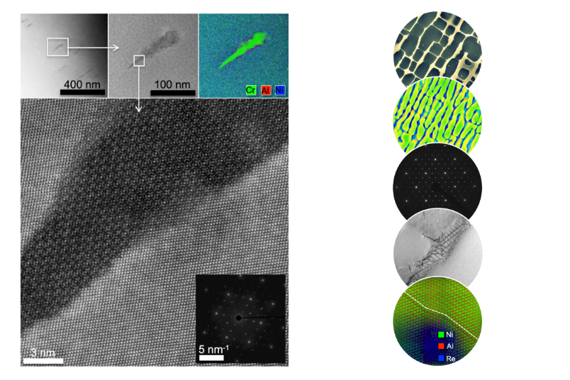
Microstructure refers to the microscopic description of the individual constituents of a material like the crystal structure (type and arrangements of atoms in a unit cell), chemical composition, size and morphology of grains, their crystallographic orientation (texture), presence of defects, their types, densities, and interactions. During fabrication and processing - the microstructure evolves, and its components interact affecting the macroscopic behavior and physical properties. Knowing the microstructure is essential for the development, optimization, and safe use of advanced materials. One of the ultimate tools for microstructural characterization is a transmission electron microscope (TEM). TEM is a research device which use an electron beam (which is transmitted through a specimen) to form an image. However, here is the most unique feature of the TEM: interacting with the ultrathin specimen electron beam cause simultaneous formation of two distinctive images: (i) a conventional image – forming in the image plane of the objective lens and (ii) an electron diffraction pattern forming in the back focal plane of the objective lens. That is up to the microscope operator to select which of the images are to be displayed and recorded for further analysis. It means that we can record an image showing us a grain, crystal or defect and a corresponding electron diffraction pattern which is essential for a detailed description of the analyzed feature. Modern instruments offer large variety of imaging modes: BF, DF, TEM, HR-TEM, BF-STEM, DF-STEM, NBD, CBED, spectroscopy modes: EDS, EELS, and 3D tomography, providing information about the structure and chemistry of the analyzed material. Often, many of these signals can be recorded simultaneously.
First electron microscope (build in 1936) offered resolution lower than that of light microscopes (light microscope resolution is typically about 200nm). Within next decades electron microscopes developed to the sub-angstrom resolution (below 70pm). That supreme resolution together with the wide range of structural information availability makes modern TEM’s a high-end tool for the advanced characterization. Advanced characterization of material is fast (to minimize the beam damage and specimen drift), precise (often the focused ion mill (FIB) prepared samples contain carefully selected microstructural features to be analyzed), and detailed (the instrument can simultaneously record signals from many detectors, or many complementary techniques is used to deliver best possible structural information).
Advanced microstructural characterization supported by scale bridging modelling is implemented to manufacturing, processing, and testing leading to better understanding of fundamental processes govern the service of advanced interface-controlled materials. Many excellent examples of advanced material characterization are published through the Collaborative Research Centre (CRC) Transregio 103 “From atoms to turbine blades – a scientific basis for a new generation of single crystal superalloys”.
