- Ruhr-Universität Bochum

Crafting quantum dots with molecular beam epitaxy
Molecular Beam Epitaxy (MBE) is a sophisticated thin-film deposition technique enabling the precise growth of crystalline structures. In MBE, beams of atoms or molecules are directed onto a heated substrate in an ultra-high vacuum, creating high-purity semiconductor materials with sub-atomic layer control. This precision makes MBE ideal for fabricating advanced nanostructures, including quantum dots (QDs).
Quantum dots are nanoscale semiconductor structures that confine electrons and holes in three dimensions, resulting in size-dependent quantum confinement effects. These “artificial atoms” exhibit discrete energy levels and can emit high-quality single photons, making them promising candidates for various quantum technologies, including computing, communication, and sensing.
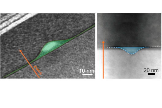
Epitaxial QDs grown by MBE have gained significant attention across engineering, materials science, physics, and quantum information technologies. Two self-assembly processes stand out in particular: Stranski-Krastanov (SK) growth and local droplet etching (LDE) (Figure 1). SK growth relies on strain-induced self-assembly, resulting in the formation of tiny islands approximately 10 nm in size. A prominent example of this technique is the growth of InAs QDs on GaAs substrates, where the lattice mismatch induces the necessary strain. In contrast, the LDE method involves the creation of nanoholes through metal droplet etching, followed by potentially strain-free QD growth. A notable example of this approach is the formation of GaAs QDs within an AlGaAs matrix, where the similar lattice constants minimize strain. Both techniques produce high-quality QDs suitable for a wide range of quantum experiments and applications, making them indispensable in the advancement of quantum technologies.
Dr. Arne Ludwig and his team have been at the forefront of developing MBE-grown InAs and GaAs QDs for such quantum experiments and applications. Their work focuses on creating ultra-low-noise InAs and GaAs quantum dots [2, 3], while improving ensemble homogeneity and density [4]. Self-assembly processes are inherently subject to random statistical fluctuations, which influence the properties of the resulting assembled particles. A key concept in understanding and controlling this phenomenon is the Voronoi cell, as described by Löbl et al. [5]. The size of these Voronoi cells plays a crucial role in determining the dimensions of the quantum emitters. By gaining control over the Voronoi cell size, one can effectively manipulate the size of the quantum emitters, offering a pathway to more precise and tailored quantum dot fabrication.
A critical hurdle in quantum dot fabrication, particularly for achieving high device yield, is the precise control of QD density and properties across an entire wafer. This challenge arises because even minute fluctuations in growth flux can result in significant and nonlinear variations in the resulting QD density [6].
Our recent research has shed light on a crucial aspect of this process: the growth phase in epitaxial QD formation [4]. This phase represents a universal characteristic of layer-by-layer epitaxial growth and can be leveraged to alter nucleation, density, and emitter properties.
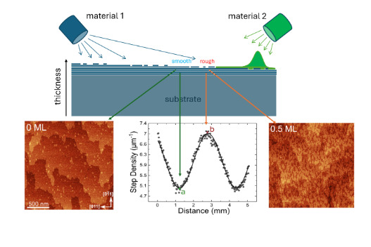
We demonstrated the significance of the growth phase in modulating the QD density [4]. Through the growth of material gradients, we generate variations in material thickness across the substrate (Figure 2). Given the discrete nature of atoms, this process naturally results in alternating regions of integer (smooth) and non-integer (rough) atomic layer thicknesses. These surface roughness modulations effectively modify surface diffusion and thus directly influence the characteristics of Voronoi cells, which are crucial in determining the spatial distribution and properties of quantum dots. Using this approach, we achieved unprecedented control over QD nucleation, creating ensembles with tailored densities ranging from one to tens of QDs per μm².
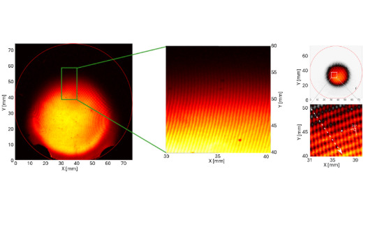
Notably, this is accomplished by substrate growth phase control without altering the nominal QD material layer thickness or composition. It is however robust to material variations occurring during full wafer growth. Our approach allows for density modulations in one and two dimensions (Figure 4), produces QDs with improved size uniformity and reduced inhomogeneous broadening, and is applicable to full wafers.
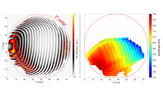
The growth phase concept extends beyond density control. Babin et al. showed it could alter the emission wavelength of LDE QDs across entire wafers [7] (Figure 3), valuable for creating QD-based devices with specific optical properties.
The implications of growth phase manipulation are far-reaching. While theoretical modelling is still in the early stage, it already opens new possibilities for designing QD-based quantum devices with precise control over emitter density and properties. This control is crucial for developing advanced multi-emitter single-photon sources for quantum communication and may find applications in photonic quantum computing, where many identical emitters are needed for complex error-proof qubit states [9].
The ability to craft QDs precisely using MBE, combined with the newfound understanding of growth phase implications, represents a significant advancement in designing functional inorganic materials for quantum technologies. Allowing the researchers to refine these techniques promises even more sophisticated quantum devices. These developments promise to accelerate the journey towards realizing practical, transformative quantum technologies that could revolutionize fields from computing to communication and sensing. The future of quantum materials science appears brighter than ever, fuelled by innovative fabrication methods and a commitment to excellence in quantum dot engineering.
The author would like to express his gratitude to all those who contributed to this research, especially Dr. Hans-Georg Babin, Dr. Nikolai Bart, and Dr. Marcel Schmidt. Special thanks to Prof. Andreas Wieck for providing his setups. The author also acknowledges the BMBF for funding the research.
References:
[1] Nguyen G. N., et al., Physical Review Letters (2023), 131, 210805.
[2] Zhai L., et al., Nature Communications (2020), 11, 4745.
[3] Ludwig A., et al., Journal of Crystal Growth (2017), 477, 193–196.
[4] Bart N., et al., Nature Communications (2022), 13, 1633.
[5] Löbl M. C., et al., Physical Review B (2019), 100, 155402.
[6] Leonard D., et al., Physical Review B: Condensed matter (1994), 50, 11687–11692.
[7] Babin H.-G., et al., Journal of Crystal Growth (2022), 591, 126713.
[8] Kruck T., et al., Crystals (2024), 14, 714.
[9] Tiranov A., et al., Science (2023), 379, 389–393.